Recent News
NQVL Design Phase Award
October 1, 2025
CHTM Joins NSF's NQVL Pilot Projects
August 9, 2024
OSE PHD, Dr. Xuefeng Li - Wins The Outstanding Interdisciplinary Graduate Programs Award
May 10, 2024
Dr. Ali Rastegari - 2024 OSE Best Dissertation Award Winner
May 10, 2024
News Archives
Patents issued to CHTM faculty
December 21, 2016 - Compiled for CHTM

The Science & Technology Corporation at the University of New Mexico (STC.UNM or STC), has announced two new patents issued recently to teams which include faculty with the UNM Center for High Technology Materials (CHTM).
As the technology transfer and economic development organization for the University of New Mexico, STC.UNM protects and commercializes technologies developed at UNM by filing patents and copyrights and transferring the technologies to the marketplace. STC.UNM also connects companies, entrepreneurs and investors to these UNM technologies for licensing opportunities and the creation of startup companies.

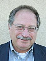
S. R. J. Brueck
U.S. Patent No. 9,520,472 was issued December 13, 2016 to Principal Investigator (PI) Steven R. J. Brueck and inventors Sueng-Chang Lee, Christian Wetzel (Troy, NY), Theeradetch Detchprohm (Troy, NY), and Christoph Stark (Neuburg, DE). The title is "Growth of cubic crystalline phase structure on silicon substrates and devices comprising the cubic crystalline phase structure."
Dr. Steven Brueck is a Distinguished Professor Emeritus with the UNM Department of Electrical & Computer Engineering (ECE), a CHTM faculty member, and Director Emeritus of CHTM. Brueck has made significant contributions to nonlinear optics, nanoscale lithography, semiconductor lasers, infrared detectors, nanophotonics and nanofluidics. He was named the STC.UNM Innovation Fellow in 2010 and received the UNM Presidential Award of Distinction in 2013. He has published over 500 technical papers and has served as an Associate Editor of Optics Letters, as Editor of the IEEE Journal of Quantum Electronics and as Founding Editor of the IEEE Journal in Selected Topics in Quantum Electronics. He holds 61 US patents of which 63 licenses and options have been exercised by 24 companies. Brueck is a fellow of OSA, IEEE, and AAAS. His most recent distinction is induction as a 2015 Fellow of the National Academy of Inventors (NAI) in Washington D.C. in Spring of 2016.
Seung-Chang Lee is an ECE Research Associate Professor and CHTM faculty member.
Abstract: A semiconductor device is disclosed. The semiconductor device includes a substrate comprising a groove. A buffer layer is formed on a surface of the groove. The buffer layer comprising at least one material chosen from AIN, GaN or AlxGa1-xN, where x is between zero and one. An epitaxially grown semiconductor material is disposed over the buffer layer, at least a portion of the epitaxially grown semiconductor material having a cubic crystalline phase structure. Methods of forming the semiconductor devices are also taught.
Source:
U.S. Patent No. 9,520,472
U.S. Patent No. 9,521,346 was issued December 13, 2016 to inventors Sanjay Krishna, Payman Zarkesh-Ha, and Glauco Rogerio Cugler-Fiorante (PI) (Sao Paulo, BR). The title is "Spatio-Temporal Tunable Pixels ROIC for Multi-Spectral Imagers."
Dr. Krishna has recently been a UNM Professor and Regents Lecturer for the UNM ECE Department with an Endowed Chair in Microelectronics; and he is the outgoing Director of CHTM. He is an SPIE, IEEE and OSA Fellow. Dr. Krishna has authored/co-authored more than 80 peer-reviewed journal articles, over 50 conference presentations, four book chapters and has ten issued patents.

Payman Zarkesh-Ha
Dr. Zarkesh-Ha is an Associate Professor with the UNM Department of Electrical and Computer Engineering, where he conducts research on interconnect predictive models to understand the limitation and opportunities for nanoscale VLSI technology. In addition, his research interests include: Statistical modeling of VLSI systems, design for manufacturability and reliability, low-power and high-performance analog and digital VLSI systems design. Dr. Zarkesh-Ha has published over 60 refereed papers and holds ten issued patents in this field. He is currently serving as technical committee member of System Level Interconnect Prediction Workshop (SLIP) and International Symposium on Quality Electronic Design (ISQED).
Abstract: Provided is a readout integrated circuit (ROIC). The ROIC includes a memory for each of a plurality of pixels, an address selector to synchronize a subsequent bias voltage for each of the pixels, a reference voltage recover switch to subtract the initial bias voltage from an output voltage of the integrated circuit and to result an integrator voltage for a sample and hold block, and a pulse-width control circuit to prevent crosstalk of the subsequent bias voltage between first and second ones of the pixels while a pixel clock selects adjacent columns. The memory maintains an initial bias voltage for each pixel during an initial integration frame time and during a sample and hold readout processing time. The sample and hold readout processing time is utilized to write a subsequent bias voltage for each pixel for a subsequent integration frame time to allow the first one of the pixels to have a different bias voltage than the second one of the pixels inside each integration frame time.
Source:
U.S. Patent No. 9,521,346


