

Recent News
NQVL Design Phase Award
October 1, 2025
CHTM Joins NSF's NQVL Pilot Projects
August 9, 2024
OSE PHD, Dr. Xuefeng Li - Wins The Outstanding Interdisciplinary Graduate Programs Award
May 10, 2024
Dr. Ali Rastegari - 2024 OSE Best Dissertation Award Winner
May 10, 2024
News Archives
U.S. Patent issued to Lee et al. for “Selective nanoscale growth of lattice mismatched materials”
June 26, 2017 - CHTM
The U.S. Patent & Trademark Office (USPTO) issued U.S. Patent No. 9,685,324, titled “Selective nanoscale growth of lattice mismatched materials,” to Lee et al. on June 20, 2017. UNM Center for High Technology (CHTM) faculty members Seung Chang Lee, principal investigator, and Steven R. J. Brueck, co-inventor, were named on the patent.
Abstract
Exemplary embodiments provide materials and methods of forming high-quality semiconductor devices using lattice-mismatched materials. In one embodiment, a composite film including one or more substantially-single-particle-thick nanoparticle layers can be deposited over a substrate as a nanoscale selective growth mask for epitaxially growing lattice-mismatched materials over the substrate.
Background
High quality epitaxial growth of heterostructures with large lattice mismatched materials is desirable for next generation electrical/optoelectronic devices and multi-functional integrated circuits. Conventional attempts to grow heterostructures such as GaAs on Si with misfit f of about 4.2%, involve methods of using: low-high two step growth with thermal cycling; post growth annealing; strained superlattice buffers; and growth on 2.degree.-off Si(001) and patterned substrates.
Nano-patterned growth (NPG), supported by the Luryi-Suhir model [see Appl. Phys. Lett. 49, 140 (1986)] has been suggested as a potential solution to lattice-mismatched heteroepitaxy. As a result, conventional NPG uses interferometric lithography and dry etching, by which In.sub.0.06Ga.sub.0.94As/GaAs heteroepitaxy (f.about.0.4%) has been formed with a pattern period of 335 nm. While there is some controversy about the validity of the model, theoretical calculations suggest that increased misfit in the NPG requires pattern structures smaller than .about.100 nm for strain relief without formation of misfit dislocations. However, this scale is beyond the reach of many of large-area lithography techniques.
There remains a need for materials and methods for forming devices over large areas with lattice mismatched materials that are strain-relieved, and have low numbers of defects. Further, while some of currently available lithography techniques such as immersion interferometric lithography may provide a desirable small scale, a need remains for alternative methods to eliminate conventional lithographic processes along with the associated etching and hydrocarbon cleaning steps to simplify the manufacturing process and to reduce the manufacture cost.
Inventors
Seung Chang (S.C.) Lee is a Research Associate Professor with the UNM Department of Electrical and Computer Engineering and with CHTM.
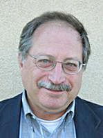
S. R. J. Brueck
Steven R. J. Brueck is a Distinguished Professor Emeritus with the UNM Department of Electrical & Computer Engineering (ECE) and Director Emeritus of CHTM. Brueck has made significant contributions to nonlinear optics, nanoscale lithography, semiconductor lasers, infrared detectors, nanophotonics and nanofluidics. He was named the STC.UNM Innovation Fellow in 2010 and received the UNM Presidential Award of Distinction in 2013. He has published over 500 technical papers and has served as an Associate Editor of Optics Letters, as Editor of the IEEE Journal of Quantum Electronics and as Founding Editor of the IEEE Journal in Selected Topics in Quantum Electronics. He holds 63 US patents of which 63 licenses and options have been exercised by 24 companies. Brueck is a fellow of OSA, IEEE, and AAAS. He was recently inducted as a 2015 Fellow of the National Academy of Inventors (NAI) in Washington D.C. in Spring of 2016.