

Recent News
NQVL Design Phase Award
October 1, 2025
CHTM Joins NSF's NQVL Pilot Projects
August 9, 2024
OSE PHD, Dr. Xuefeng Li - Wins The Outstanding Interdisciplinary Graduate Programs Award
May 10, 2024
Dr. Ali Rastegari - 2024 OSE Best Dissertation Award Winner
May 10, 2024
News Archives
LESA ERC's recent patent is featured in Semiconductor Today
February 16, 2017 - Excerpted from Semiconductor Today
U.S. Patent No. 9,520,472 was issued December 13, 2016 to Principal Investigator (PI) Steven R. J. Brueck and inventors Sueng-Chang Lee, Christian Wetzel (Troy, NY), Theeradetch Detchprohm (Troy, NY), and Christoph Stark (Neuburg, DE). The title is "Growth of cubic crystalline phase structure on silicon substrates and devices comprising the cubic crystalline phase structure." Learn more about the patent here.
The research team includes faculty and graduate students at the Center for Lighting Enabled Systems & Applications (LESA) of Rensselaer Polytechnic Institute (RPI) of Troy, NY, USA and The University of New Mexico (UNM).
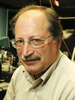
Steven R. J. Brueck
Dr. Steven Brueck is a distinguished professor emeritus with the UNM Department of Electrical & Computer Engineering (ECE), a faculty member at UNM's Center for High Technology Materials (CHTM), and director emeritus of CHTM. Brueck has made significant contributions to nonlinear optics, nanoscale lithography, semiconductor lasers, infrared detectors, nanophotonics and nanofluidics. Seung-Chang Lee is an ECE research associate professor and CHTM faculty member.
Rensselaer participants include Christian Wetzel, professor of physics, applied physics, and astronomy and co-inventor of the patent; along with Theeradetch Detchprohm, who received his Ph.D. from Japan's Nagoya University and served as a research associate professor in the Future Chips Constellation; and Christoph Stark, who received a Ph.D. in physics from Rensselaer and now works for a startup company in Germany.
"The patented UNM/RPI growth process uses inexpensive silicon wafers available in much larger sizes and lower defect densities than sapphire," says Brueck. "The silicon surface is first patterned with an array of nanoscale grooves that lead to a unique, geometrically driven phase segregation that separates the cubic phase and promotes its growth at the expense of the hexagonal phase GaN (gallium nitride) material," he adds. "Additional quantum well layers of InGaAs (indium gallium arsenide) are added after the pure cubic phase GaN structure has been established to create the light-emitting material used to fabricate cubic LEDs."
By using a non-polar facet of cubic GaN, the research team has demonstrated emission across the visible spectrum from the cubic InGaN/GaN material system that offers significant opportunities for higher efficiency full-spectrum lighting and displays.
The research team and other investigators are working to develop LED manufacturing processes that will allow LEDs to shine brighter and in more colors. The material could be used in applications that include lighting for homes that would create brighter, more colorful, and efficient displays, as well as high-efficiency power electronics that are used to improve electric vehicles and renewable energy system performance.
Ultimately, LESA's vision is focused on creating digitized illumination for new applications in lighting, healthcare, building management, horticulture, and advanced 5G wireless communications platforms.
Semiconductor Today is the first digital-only magazine for the compound semiconductor and advanced silicon industries. Its rapidly growing circulation comprises thousands of scientists, engineers, and executives involved in the manufacturing and R&D of compound semiconductor and advanced silicon materials and devices.
Related:
- Read the entire article at Semiconductor Today:
LESA's Lighting and Displays team at RPI and University of New Mexico awarded patent for inexpensive growth of large-area cubic GaN - Patents issued to CHTM faculty
- U.S. Patent No. 9,520,472
- “Smart Lighting” inpatient Hospital Room completed at UNM Health Center
- Smart Lighting Hospital Room at UNM HSC is ready for sleep studies