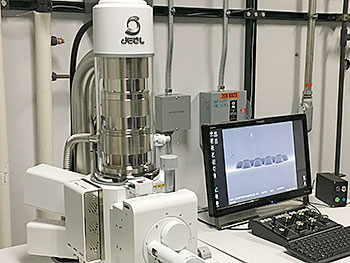
Scanning Electron Microscope (SEM)

JSM-IT100 InTouchScope™
The JSM-IT100 scanning electron microscope (SEM) is manufactured by JEOL, a leading global supplier of electron microscopes, ion beam instruments, mass spectrometers and NMR spectrometers.
Novices as well as experienced users can quickly obtain high quality images using both secondary electron and backscatter imaging.
DESCRIPTION:
The JSM-IT 100 is a simple-to-use, versatile, research-grade SEM with a compact ergonomic design. It offers high resolution imaging and a range of acceleration voltages at both high and low vacuum modes. The JSM-IT 100 is a remarkably intuitive, high throughput microscope. Fast data acquisition makes imaging and analysis of samples a simple task.
SPECIFICATIONS:
The embedded JEOL EDS system with silicon drift detector technology now includes Spectral Mapping, Multi-Point Analysis, Automatic Drift Compensation, Partial area, Line Scan, and Mapping Filter functions. It provides fast sample navigation at anywhere from 5x – 300,000x magnifications.
MATERIALS:
No restrictions within reason.
DETAILS:
To learn more about the JSM-IT 100, visit the JEOL USA webpage for specifications.
SmartEBIC system upgrade
An electron-beam-induced-current (EBIC) system has been installed as a significant upgrade to the SEM. It adds the ability to image and measure changes to a sample induced by variations in temperature or electric current.
The SmartEBIC system includes the Digiscan II system that enhances the photographic quality of images; Microscopy Suite Software; Cooling Stages model C1001 which utilizes liquid nitrogen coupled with the 1905 temperature controller; and a Stanford Research Systems Low Noise Pre-Amplifier.
EBIC is used extensively in semiconductor and photovoltaic research, and the dynamic capabilities of observing changes to a sample in real time opens up entirely new areas of semiconductor analysis at CHTM.
For more information, refer to the CHTM news article about the EBIC upgrade.


