

Crystal Growth Facility
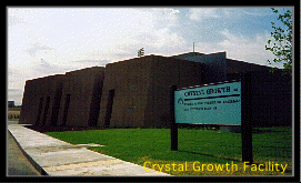 The Crystal Growth Facility (CGF) is located at 1000 University Blvd. (to the East of the main CHTM building).
The CGF was designed to house MOCVD (metalorganic chemical vapor deposition) and MBE (molecular beam epitaxy) systems for the epitaxial growth of advanced semiconductor structures for CHTM and other users. At present there is one MOCVD system and one MBE system growing GaAs, InGaAs, AlGaAs, GaN, InGaN, AlGaN and icosahedral boron compounds, for a wide range of optoelectronic and electronic device and materials. The CGF also houses essential tools for the rapid characterization of epitaxial materials (e.g. Philips MRD X-ray diffractometer and a room temperature photoluminescence set-up.)
The facility includes an integrated safety system for the continuous monitoring of hazardous materials. In the event of a building alarm this safety system automatically shuts down the reactors to a failsafe condition and notifies the appropriate persons that there is a non-standard condition.
For building issues please contact info@chtm.unm.edu
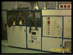 Crystal Specialties MOCVD Reactor
This MOCVD system has been adapted for high temperature MOCVD growth up to 1100 C. This horizontal geometry reactor features a rectangular flow liner and an inclined, RF-heated susceptor for improved uniformity.
This system is currently being used for the growth of GaN and InGaN alloys for a variety of materials and device projects at CHTM. We are also beginning a new program in which icosahedral borides will be grown and investigated for novel energy conversion devices.
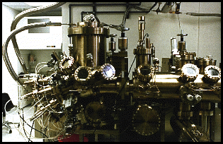 V80H MBE System
MBE (molecular beam epitaxy) deposits epitaxial films using advanced evaporation sources (known as Knudsen cells). Each source directs an elemental "beam" at the heated substrate and the simultaneous evaporation of different elements allows compound semiconductors such as GaAs, AlGaAs, GaInAs, InP, etc. to be deposited. Doping is achieved by adding a small beam flux of the required doping element. Growth rate is controlled by the beam flux and layers are stopped and started by closing and opening high speed shutters that are placed infront of the knudsen sources.
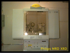 Philips MRD X-Ray Diffractometer
This high resolution XRD unit features a 4-crystal primary monochromator, a full motion goniometer and a 3-bounce analyzer crystal. The system is completely computer controlled and equipped with hardware and software accessories to perform the following measurements:
- Theta/2-Theta XRD
- Rocking curves
- Reciprocal space mapping
- Grazing incidence X-ray reflectivity (GIXR)
XRD measurements play a vital role in the improvement of crystalline quality in new semiconductor materials such as GaN.
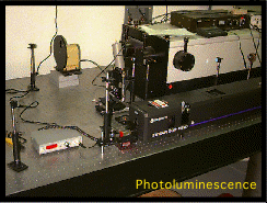 Room Temperature Photoluminescence (PL)
The bandgap of direct-gap semiconductors can be rapidly and non-destructively measured using photoluminescence. In the case of ternary semiconductor alloys, such as InGaAs, AlGaAs or AlGaN, the PL measurement provides a rapid measure of the alloy composition that can be used to verify independently the composition as measured by X-ray diffraction.
This PL apparatus has two excitation sources, a 0.5 W argon-ion source emitting at 514 nm and a doubled argon-ion laser emitting 100 mW, CW at 257 nm, which allows the PL analysis of conventional and wide-gap semiconductors, respectively. The system also features lock-in amplification for a high signal-to-noise ratio and dual detectors to cover a full wavelength range