

Recent News
NQVL Design Phase Award
October 1, 2025
CHTM Joins NSF's NQVL Pilot Projects
August 9, 2024
OSE PHD, Dr. Xuefeng Li - Wins The Outstanding Interdisciplinary Graduate Programs Award
May 10, 2024
Dr. Ali Rastegari - 2024 OSE Best Dissertation Award Winner
May 10, 2024
News Archives
Scanning Electron Microscope upgrade adds observation of changes to a sample with variations in temperature or electric current
February 17, 2017 - Sharon Steely
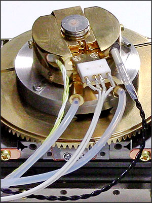
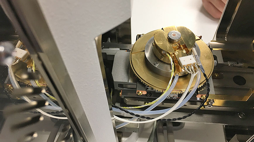
EBIC device installed on SEM sample plate
An electron-beam-induced current (EBIC) system has been installed as a significant upgrade to the JEOL JSM-IT100 Scanning Electron Microscope (SEM) in the SEM Lab at UNM's Center for High Technology Materials (CHTM). The SmartEBIC system adds new dimensions to the magnification capabilities (up to 300,000 X) of the SEM. It enables dynamic experiments, providing much more information on a sample than available with previous techniques.
"EBIC is used extensively in semiconductor and in photovoltaic research. With the ability to image and measure changes to a sample induced by variations in temperature or electric current, this upgrade opens up entirely new areas of semiconductor analysis at CHTM."
— Tito Busani, Nanofabrication Operations Manager, CHTM
CHTM acknowledges the sponsorship of the Air Force Research Laboratory through SK Infrared for this upgrade. The SmartEBIC system is a significant addition to materials characterization capability at CHTM that will enable UNM students to extend their research, as well as enhancing CHTM's collaboration with our partners, including University of Texas at Austin and Sandia National Laboratories.
Components of the EBIC upgrade to the SEM
The SmartEBIC system installed at CHTM also includes the Digiscan II system that enhances the photographic quality of images; Microscopy Suite Software; Cooling Stages model C1001 which utilizes liquid nitrogen coupled with the 1905 temperature controller; and a Stanford Research Systems Low Noise Pre-Amplifier.
Observing sample changes produced by electric current
Instead of looking at photons of light, as in a typical microscope, or imaging electrons hitting a sample in an SEM, the SmartEBIC system enables researchers to image and measure variances of electric current. Researchers can observe in real time the changes a current induces on their samples, as well as look at two points of electricity on a sample and watch them interact. This technique can be used for diodes and transistors, to bias the sample in certain ways. Observing how the junction is actually working provides the ability to assess the ability of a sample or diode for amplification or as a switch.
Feed-throughs for electric current are part of the EBIC device. In addition, two probes are available which can be moved to actually touch the surface of the sample. The current that is induced can be measured. The EBIC device also features a Faraday Cup, so that researchers can observe the true electron beam current in the sample chamber. This can be compared with the results of an experiment, so that the researcher can measure the properties of current absorption or rejection (conductivity) of the sample.
Observing samples at temperatures from -185°C to +100°C
The Gatan Cooling Stages system can chill a sample down to to less than -185°C in just a few minutes. The researcher can observe the changes to the characteristics of the sample over the range of temperatures. One of the advantages to producing very cold temperatures for an experiment is that beam-sensitive materials are stabilized under high beam currents. The characteristics of a semiconductor can change with temperature. For some to run at peak efficiency requires very cold temperatures.
Stabilizing the sample chamber to room temperature after a chilled sample takes much more time, so planning experiment sessions must be done with this in mind. This device can also heat samples up to +100°C. Extreme care must be taken not to add samples that melt under this kind of heat, which would coat all of the surfaces and devices in the sample chamber. If there is water vapor in the chamber, ice can possibly collect on the sample.
User notes
EBIC is a powerful technique to image the electrical properties of semiconductors in conjunction with their structural properties. To generate an EBIC image, a SEM column is used to generate an electron beam, which is swept across a sample. The system is capable of creating a visual representation of the electrons that are collected in terms of brighter and darker areas (non-collected electrons) at a specific junction. The SEM system then generates an image of the sample and the junctions, which can be superimposed with the current image from the EBIC. In this manner, CHTM researchers can visually show where the current (electrons) are accumulated and the electrical quality of the junction.
— Tito Busani, Nanofabrication Operations Manager, CHTM
The scanning electron microscope (SEM) in the electron beam induced current (EBIC) mode is used to characterize semiconductor materials. In this technique, the electron beam generates charge carriers near the p-n junction and currents induced by the junction’s built-in electric field are measured. The result will be a spatially resolved map of the diode’s response, and when the measurement is performed at different beam energies, it helps get additional data to fit parameters such as the bulk minority carrier lifetime, carrier’s diffusion length and the surface recombination rate. EBIC offers a more detailed analysis of semiconductor devices, which can be of great benefit to students and researchers at CHTM.
— Zahra Taghipour, doctoral student, Optical Sciences & Engineering
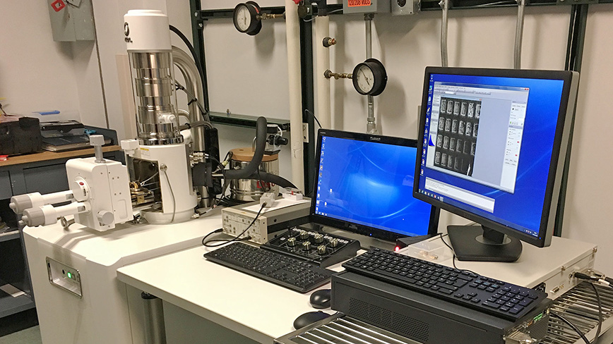
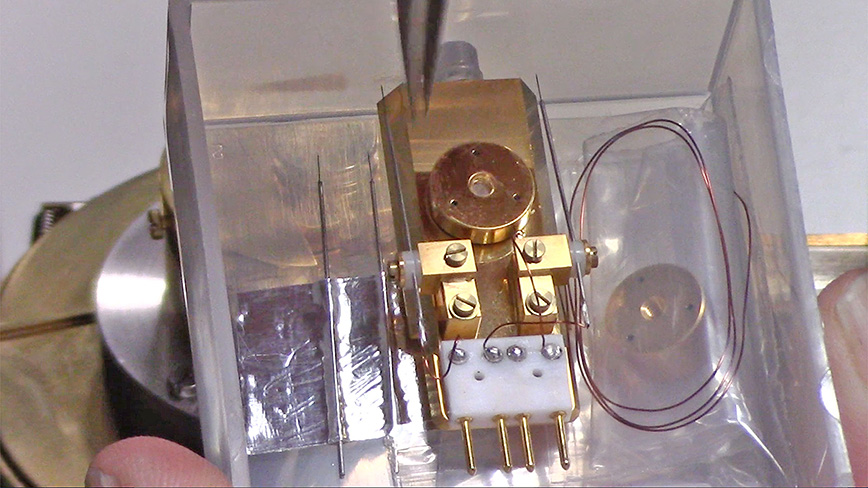
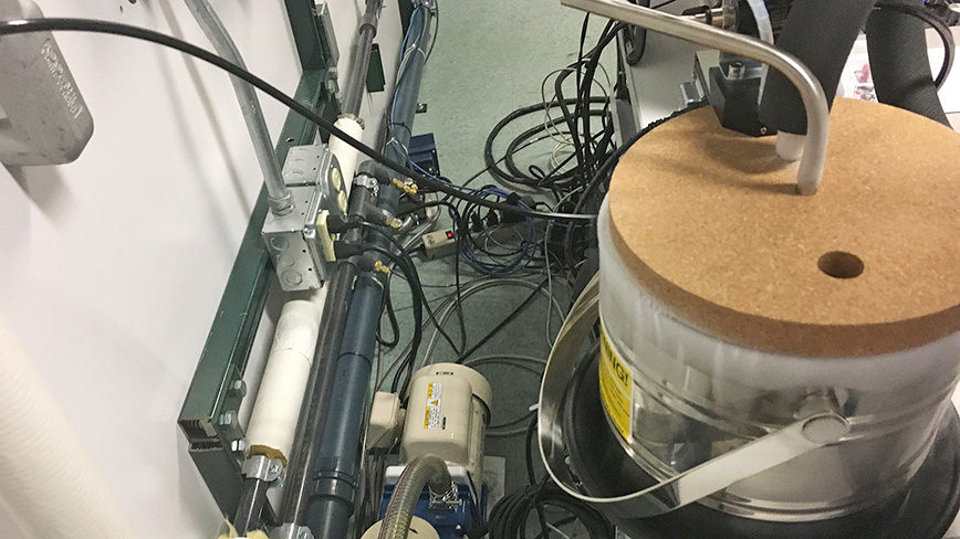
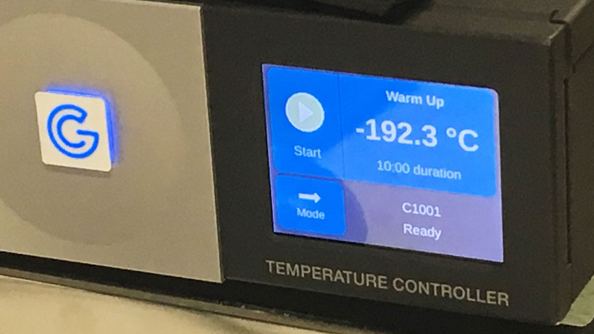
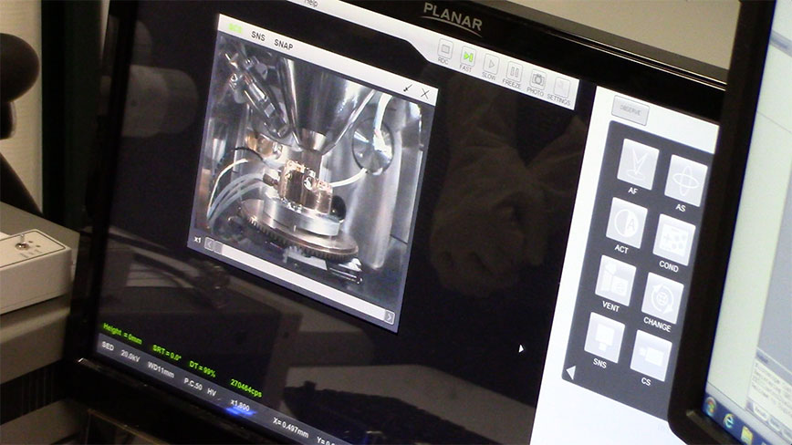
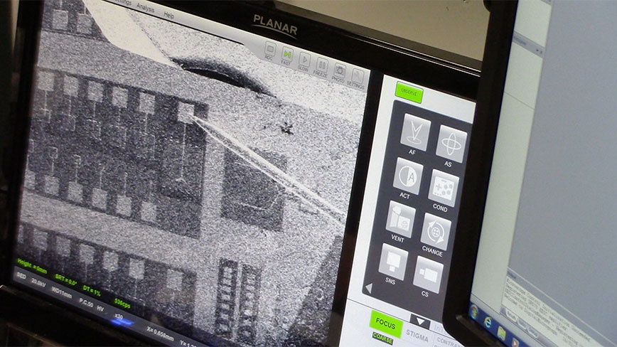
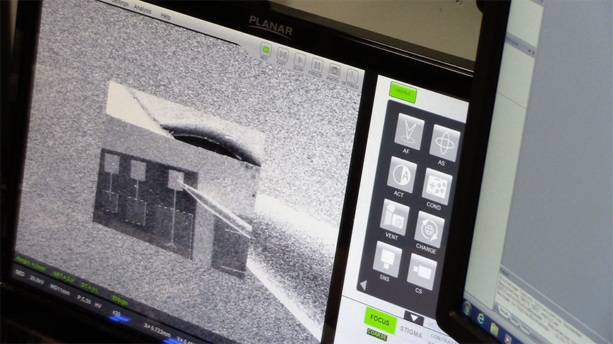
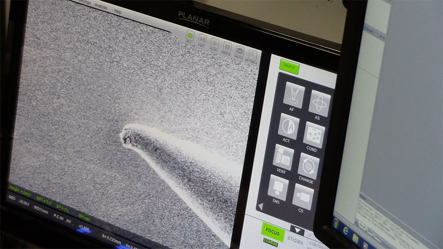
View of the SmartEBIC components installed in the SEM Lab shows the second monitor displaying the Microscopy Suite Software, the Digiscan II, the Temperature Controller, and the Low Noise Pre-Amplifier. The SEM sample chamber is open, and the EBIC device is shown installed on the SEM sample plate. Then, a closeup of the EBIC electrical kit shows the feed-through contacts, probes, and the three holes in the EBIC sample plate that create the Faraday Cup. The nitrogen delivery system has brought the sample temperature down to -192.3 degrees Celsius.
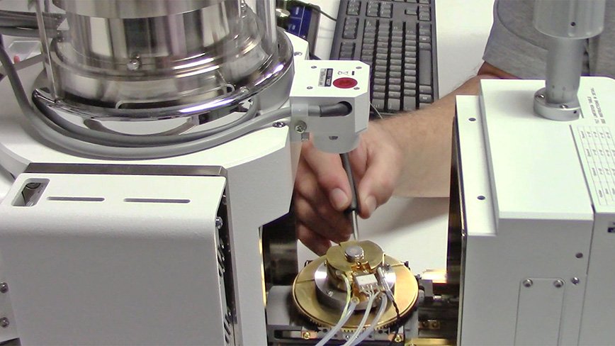
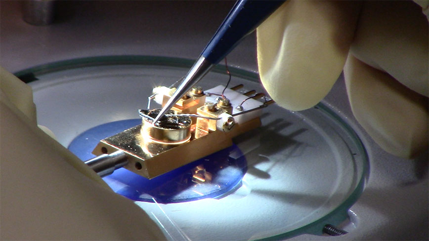
Finally, a CHTM graduate student learns how to place the EBIC device's probes in contact with a sample, using a microscope to assist in positioning. Then, the probe in contact with the semiconductor sample is imaged on the Digiscqn II system, starting with an interior view of the sample chamber.